Solid State Chemistry and Mechanochemistry
of the Siberian Branch of the Russian Academy of Sciences (ISSCM SB RAS)
Developments / New materials
ELECTROCONDUCTING POWDERS OF METAL NANOPARTICLES FOR ADDITIVE TECHNOLOGIES
Electroconductive materials have been developed that can be used as ink for piezo-jet printing in specialized research and industrial inkjet printers in the formation of electrically conductive elements and coatings on flat substrates in order to create functional materials and devices in electronics, instrumentation, aviation, space technology and other fields.
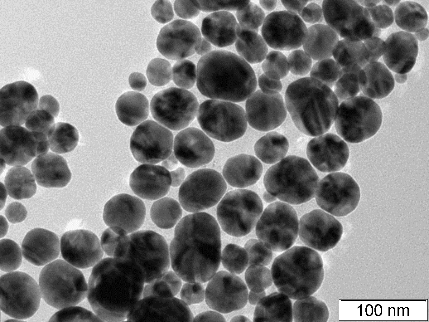
Electroconductive materials are a dispersion of surface-modified metal nanoparticles (silver, copper, nickel) stabilized in an organic solvent obtained by extraction-polyol method, with an average size of less than 50 nm.
The technology for obtaining metal nanoparticles is protected by Russian patents.
Advantages of materials
- High content of metal nanoparticles (more than 50 mass%).
- Low cost due to the simplicity and efficiency of the method of synthesis of metal nanoparticles.
- High stability of materials (more than 6 months).
- Compatibility of ink with industrial printheads such as Konica Minolta, Xaar, Rico, etc.
Application
- in photovoltaics to create electrically conductive contacts in the manufacture of solar cells,
- in the manufacture of OLED displays and light sources, chemical sensors,
- for the prototyping of printed circuit boards, the metallization of ceramic products, the manufacture of RFID antennas,
- metal nanoparticles can also be used to fabricate electrically conductive composite materials - pastes, adhesives, polymers.
Contact us:
Institute of Solid State Chemistry and Mechanochemistry SB RAS
Kutateladze str., 18 Novosibirsk, 630128 Russia
Phone: +7(383)332-53-44
Fax: +7(383)332-28-47
E-mail: root@solid.nsc.ru
Institute of Solid State Chemistry and Mechanochemistry of SB RAS


